Rigid Flex HDI PCB , Flexible PCB (FPC)
Argus Systems (AESPL) is leading Flexible PCB (FPCB) and Rigid Flex PCB manufacturer in india providing high quality multi-layered Rigid Flex HDI PCB, Flexible PCB (FPCB), Flexi Rigid PCB, HDI PCB & RF PCB solutions for Aerospace & Defense (AS9100D, MIL-PRF Military grade PCB, LCSO), Medical (ISO 13485),Automotive (IATF 16949 )and industrial applications.
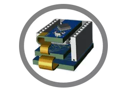
Flex PCB (FPCB) and Rigid Flex HDI PCB
- Flexible printed circuit (FPC) Boards and Rigid Flex HDI PCB circuitry provides a means to integrate multiple PCB assemblies without wires, cables or connectors, replacing them with thin, light composites that integrate wiring in ultra-thin, flexible ribbons between sections.
- In flex Rigid PCB packaging, a flexible circuit substrate provides a backbone of wiring with rigid multi-layer circuit sections built up as modules where needed.
- Flexible PCB (FPC) & Flex Rigid PCB has improved resistance to vibrations and movement, Small package size, High tensile strength, High bendiness and suitability for harsh environments.
- Single sided flexible material with or without shield or stiffener .
- Double sided flexible material with or without shield or stiffener with plated through holes.
Flex PCB and Rigid-Flex PCB
- Multilayer flexible material with or without shield(s) or stiffener (more than two conductor layers) with plated through holes and HDI.
- Multilayer rigid and flexible material combinations (more than two conductor layers) with plated through holes and HDI.
- 1-20 layers flex Rigid PCB
- Rigid-Flex PCB with Dimensions up to 24" x 48".
- Thickness up 0.125".
- 4/4 mil line width/spacing.
- FR4 material for Rigid core & Prepreg.
- Acrylic, epoxy, and adhesiveless polyimide flex materials.
- Dupont Material for Flex core, Coverlay film and flex adhesive.
- Bikini cut, bookbinder, loose-leaf construction.
High Density Interconnect PCB
- High Density Interconnect PCB Design use latest PCB manufacturing technologies available to increase the functionality of PCBs using the same or less amount of area.
- HDI PCBs are characterized by high-density attributes including laser microvias, fine lines and high performance thin materials. This increased density enables more functions per unit area.
- 1+N+1 - PCBs contain 1 "build-up" of high-density interconnection layers.
- i+N+i (i≥2) - PCBs contain 2 or more "build-up" of high-density interconnection layers.
- Any Layer HDI - All the layers of a PCB are high density interconnection layers which allows the conductors on any layer of the PCB to be interconnected freely with copper filled stacked microvia structures ("any layer via").
- 2/2 mil line/space with 4/8 mil laser via capture pad size.
- Material options:High temperature FR4, Halogen – Free and High Speed (low loss).
HDI PCB Microvias
- A microvia maintains a laser drilled diameter of (typically 0.006" , 0.005" , or 0.004" ),which is optically aligned and requires a pad diameter (typically 0.012" , 0.010" , or 0.008"), allowing additional routing density.
- Microvias can be via-in-pad, offset, staggered or stacked, non conductive filled and copper plated over the top or solid copper filled or plated.
- Microvias on different layers can be staggered or stacked.
- Microvias add value when routing out of fine pitch BGAs such as 0.8 mm pitch devices and below.
- Standard Microvias limited to layers 1-2 & 1-3.
- Additionally, microvias add value when routing out of a 0.5 mm pitch device where staggered microvias can be used.
- Routing micro-BGAs such as 0.4 mm, 0.3 mm, or 0.25 mm pitch devices, requires the use of Stacked MicroVias using an inverted pyramid routing technique.
HDI PCB Stacked MicroVias
- Higher technology HDI PCBs have multiple layers of copper filled stacked microvias (Advanced HDI PCBs) which creates a structure that enables even more complex interconnections.
- Stacked MicroVias Allows increased routing on multiple layers as Standard Microvias limited to layers 1-2 & 1-3.
- Stacked MicroVias Provides routing solutions for next generation small pitch packages of 0.5/0.4/0.3/0.25 mm.
- Stacked MicroVias Provide solid copper plate eliminating potential solder voiding.
HDI PCB Deep Microvias & Deep Stacked MicroVias
- Deep Microvias & Deep Stacked MicroVias have Improved Impedance performance.
- Provide additional dielectric material.
- Maintains small geometries on multiple layers.
- Improved signal integrity.
- Provides RF Microvia solutions.
- Provides a solid copper plate.
- Improves Current Carrying Capability & Thermal Management.
- Provides a Planar surface for BGA (Via-in-Pad).

Rigid , Flex RF & Microwave PCB
- Selective plated up layers.
- Exact registration/laser direct imaging.
- Front to back registration of etched cores.
- Mixed Dielectric constructions.
- Buried / Blind / Microvia.
- Multilevel cavity constructions.
- Optical mill / drill, Laser routing.
- Back Drill for Precision Stub Removal.
- Sequential lamination.
- Plated edges.
- Hole Fill (Conductive, nonconductive, and partial hole fill options).
- Surface Finishes (ENIG, ENEPIG, Hard and soft wire bondable gold, Immersion silver).
RF & Microwave PCB
- Microwave & RF PCB manufacturer with advanced engineering and process capabilities.
- Wide range of low loss laminates and resin systems.
- Supports a wide range of frequency bands (L, S, C, X, Ku, K, Ka, V, W) for aerospace & Defense electronics, medical devices, Automotive ADAS, networking and telecommunications equipment.
- High Power RF PCB Thermal Solutions include Copper coins and slugs, Metal Core & Metal Back, and Thermally conductive laminates.
Reach out to your Application Engineering Team to Discuss Your PCB requirements for flexible hybrid electronics.
Argus Systems (AESPL) a globally recognized PCB Design, PCB fabrication and PCB assembly company supporting Fabrication of Flexible PCB, Rigid Flex HDI PCB, HDI PCB, RF PCB and flexible hybrid electronics for Its Global Clients in India, USA, UK, Germany, France, UAE, Saudi Arabia, and Australia as per Automotive ( IATF 16949 ), Medical Devices (ISO 13485), Aerospace & Defense (AS9100D, MIL-PRF Military grade PCB, LCSO) quality management standards.