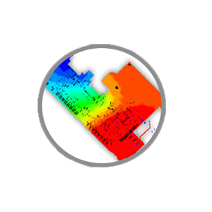
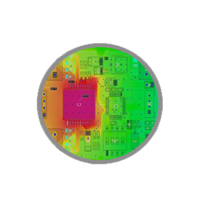
PCBA Thermal Simulation and PCB Thermal Analysis Services
Argus Systems (AESPL) provides advanced PCB thermal simulation services and PCB thermal analysis services for high-performance electronic systems. Our solutions help optimize heat dissipation, improve reliability, and enhance overall system performance.
We specialize in PCBA thermal simulation and system-level thermal engineering for industries such as aerospace, avionics, telecom, industrial, medical, and automotive. Our services ensure efficient thermal management and long-term product stability.
In addition, we offer signal integrity (SI), power integrity (PI), crosstalk analysis, EMI/EMC analysis, and reliability engineering to support complete electronic system design and validation.
A growing number of companies are experiencing a sharp upturn in system-level Signal Integrity, Power Integrity,Thermal, EMI EMC and Reliability issues that result in project delays and increased cost.Many companies do not have in-house expertise and the companies that do have the expertise may experience peak overloads that require periodic outsourcing. Argus quick turn design analysis services address the needs of these customers by providing expert resources at very affordable prices.
System level thermal constraints
- Local ambient temperature at the Component.
- The airflow over the component and surrounding board.
- Physical constraints at, above, and surrounding the component which may limit the size of a thermal enhancement (for example heat sink).
- System design should consider enough Holes or slits in enclosure for better ventilation.
Component’s level thermal constraints
- Component power dissipation.
- Component size and packaging materials (effective thermal conductivity).
- Type of interconnection to the substrate and the board.
- The presence of a thermal cooling solution.
- Thermal conductivity and the power density of the substrate, nearby components, and the board.
Thermal Design Parameters
Component related parameters
- The value of θjc and θja taken from package thermal datasheet.
- The value of θja for air-cooled systems should be specified for at least two values of airflow.
- Maximum permissible operating temperature for the case and junction as specified in the device datasheet.
PCB Related Parameters
- Board dimension.
- Copper, dielectric and total Board thickness.
- Thermal conductivity of dielectric, copper and any coating finishing material.
- Thermal heat pads.
- Interface material used for efficient heat transfer.
- Thermal via.
Power dissipation
- The device power has to be estimated looking at the circuit functionality, operating frequency (in case of devices which are clocked), duty cycle, load it is driving.
- The maximum power dissipation that is given in the data sheets should not to be taken as the operating power.
- Power dissipation for Voltage Regulators, DC-DC Converters is based on their efficiency (as per device data sheet). Normally 75% to 85% efficiency might be considered for arriving at power dissipation.
- Power dissipation for all passive capacitors.
- Power dissipation for resistors (based on the circuit functionality).
- Power dissipation for zener diodes (based on circuit functionality).
Operating Parameters
- The thermal characteristics of the PCB are dependent on position of the board in the system, and its construction.
- Mounting of the boards: in a rack or as a single board.
- Component mounting on the board: one side or both the sides.
- System and board level cooling - forced air cooled or conductive cooled.
- In a rack-mounted assembly position of the board: middle or edges.
- If the board is mounted inside a rack, power dissipation of either side of the card should be taken in consideration for effect of radiated heat.
- Edges of the rack should be modelled as being maintained at the ambient temperature.
- All heat sinks and thermal sinks.
PCB layout aspects for improving thermal performance
Thermal Tab for Components
- Electrically connect Thermal Tab/Heat Lugs of devices to ground or output (as per device datasheet).
- Create copper plane below the Heat lugs on component and solder side.
- Open the copper plane (no solder mask) below Heat lugs. Make this copper plane area as large as permitted by layout.
- Stitch the Top and bottom copper pouring together using thermal vias to reduce thermal resistance.
- This copper pour stitching should be done to internal power plane as well if it’s electrically connected.
- Use more number of bigger stitching vias for reduced thermal resistance.
- Fill all thermal vias with solder material to improve thermal conductivity.
Thermal enhancements
- Thermally conductive material choterm might be added in the gap b/w board surface and the component bottom surface.
- Holes could be added under IC if possible (This Hole should be modelled as via filled with solder for thermal analysis).
- Layout should consider providing an option for Heat sinks if thermal analysis results indicates necessity of thermal enhancements.
- If Metal stand-off installed on the mounting holes are part of metal case it could help in heat dissipation. Connect mounting hole to copper pour to take advantage of this.
- Shut-down unused peripherals to cut down on heat dissipation as well runs peripherals at lower clock frequency enough to meet performance benchmarks.
Copper pouring
- Thermal performance of the board can be increased further by increasing the copper percentage of the board.
- It is suggested to pour copper where ever is possible on both top and bottom layer to spread the heat over the board.
- Copper pour used under IC’s should be modelled as conduction pads to provide heat dissipating path.
- If copper is poured in both and top layer (and both are electrically connected to same power net) then stitch these pouring using vias.
- This copper pouring could be stitched to internal power plane if it’s electrically connected.
- Use 1 Oz (or more) copper plane on solder side.
Component Placement
- Consider a component Placement plan which scatters warm parts through out the board compared to heat producing components in a group. For example avoid placing liner regulators close to processors which typically dissipates ~2W or more.
- Even if two parts are symmetric, the part which is placed close to board edge would be hotter than the one which is placed well inside the board edge. The component placed towards board edge can only dissipate heat in one way (through PCB) and as a result could be hotter.
- Board size might be increased or placement might be adjusted to put more space around warm parts.
Argus Systems a globally recognized PCB Design and electronic manufacturing company Providing hardware system design, Electronics Hardware design, PCB layout design and product design analysis (PCB Signal Integrity Analysis , PCB Power Integrity Analysis ( PI Analysis) , PCB Thermal Simulation, PCB Thermal Analysis, Reliability Analysis , PCB EMI EMC Simulation ,PCB EMI EMC analysis , PCB Crosstalk Analysis) to Its Global Clients in India , USA, UK, Germany, France, and Australia for Automotive, Medical, Aerospace & Defence and Industrial applications.